Electronics Notes - Devices, Circuits, Systems, and Implementation
This note is adapted from course materials for EE2005 Electronic Devices and Circuits at City University of Hong Kong. Instructor: course teaching staff.
Central Question
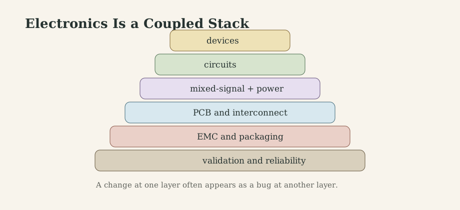
Electronics asks: how do we control charge, energy, information, and heat through real components that are never ideal?
The same circuit must satisfy equations, tolerances, layout constraints, measurement limits, thermal limits, electromagnetic compatibility, and manufacturability. Good electronics design is therefore a chain from device physics to system validation.
1. Circuit Models and Conservation Laws
Kirchhoff’s laws are conservation statements:
- KCL tracks charge continuity at nodes,
- KVL tracks energy consistency around loops.
Nodal analysis writes these constraints as algebra:
\[\sum_k \frac{V_i-V_k}{R_{ik}}+I_{source,i}=0.\]Thevenin and Norton equivalents separate source behavior from load behavior:
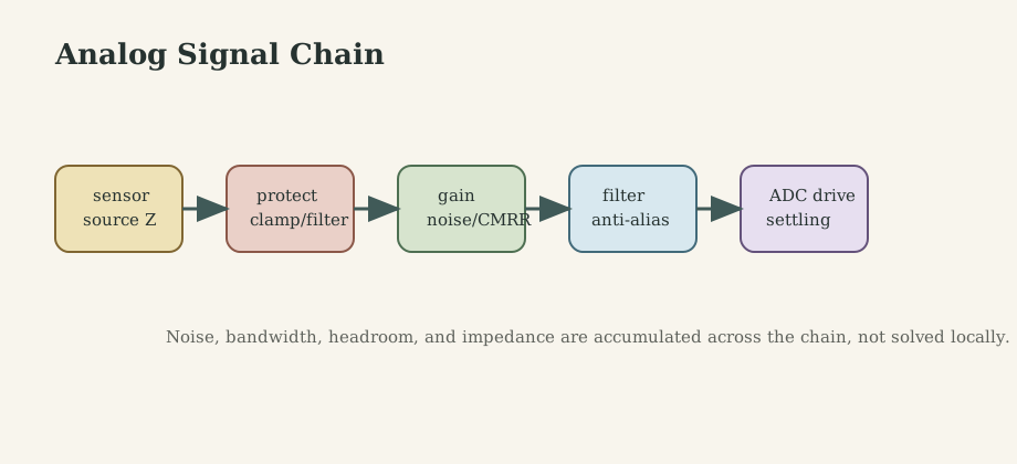
\[V_{TH}=V_{OC}, \qquad R_{TH}=\frac{V_{OC}}{I_{SC}}, \qquad I_N=\frac{V_{TH}}{R_{TH}}.\]This modular viewpoint is practical: sensor front ends, filters, amplifiers, ADC inputs, and cables all interact through source and load impedances.
Capacitors and inductors turn circuits into dynamic systems:
\[C\frac{dv}{dt}+\frac{v}{R}=i(t), \qquad L\frac{di}{dt}+Ri=v(t).\]The first engineering habit is to write assumptions near the first equation: small-signal, quasi-static, room-temperature, ideal supply, negligible parasitics, or single-frequency operation. Most lab surprises are broken assumptions rather than mysterious physics.
2. Diodes, Transistors, and Bias
The diode is a nonlinear, temperature-sensitive element. Shockley behavior gives the baseline:
\[I_D=I_S\left(e^{V_D/(nV_T)}-1\right), \qquad V_T=\frac{kT}{q}.\]In real designs, series resistance, reverse recovery, leakage, junction capacitance, energy rating, and layout inductance matter. A TVS diode placed far from the connector may clamp too late because the trace inductance creates voltage overshoot.
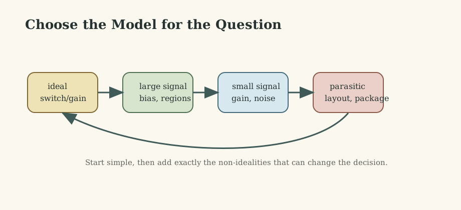
BJTs and MOSFETs provide controlled current flow, but their useful models depend on operating region. For a BJT in active operation:
\[I_C\approx I_Se^{V_{BE}/V_T}, \qquad g_m=\frac{I_C}{V_T}.\]For a long-channel MOSFET in saturation:
\[I_D\approx \frac{1}{2}\mu C_{ox}\frac{W}{L}(V_{GS}-V_{TH})^2(1+\lambda V_{DS}).\]Bias networks should not rely on a single nominal parameter such as $\beta$ or threshold voltage. Robust design checks process, voltage, temperature, and load corners.
3. Analog Amplifiers and Op-Amps
An amplifier is not just a gain block. It must preserve information while controlling noise, distortion, bandwidth, stability, loading, and headroom.
For a common-source or common-emitter stage, a useful midband estimate is
\[A_v\approx -g_m(R_{load}\parallel r_o).\]Emitter or source degeneration trades gain for linearity, bias stability, and predictability. Cascaded stages require impedance planning; otherwise one stage silently changes the pole locations of the next.
Op-amp circuits begin with ideal feedback rules but must be checked against finite open-loop gain, gain-bandwidth product, slew rate, input common-mode range, output swing, bias current, and load drive:
\[A_{CL}=\frac{A_{OL}}{1+A_{OL}\beta}, \qquad \left|\frac{dV_o}{dt}\right|_{\max}\le SR.\]For instrumentation, CMRR is a system property. Resistor matching, source imbalance, PCB symmetry, shielding, and grounding can degrade the performance of an otherwise excellent amplifier.
4. Digital Logic, Timing, and Mixed-Signal Interfaces
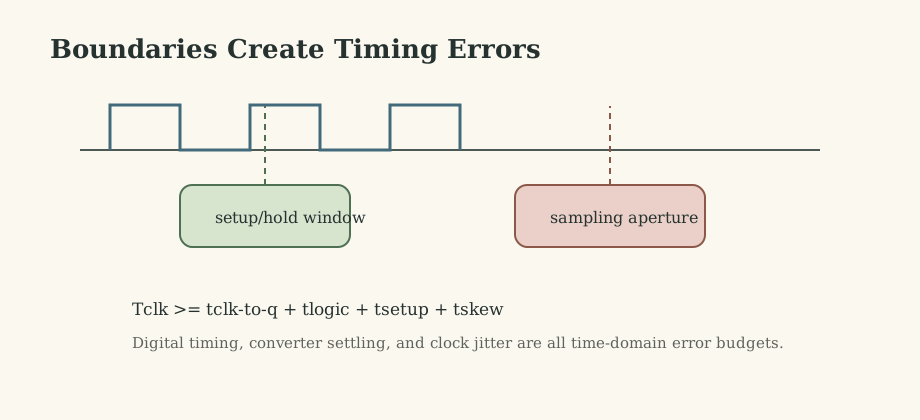
Digital systems fail when Boolean correctness is treated as the whole problem. Real logic also needs voltage margin, setup and hold timing, clock integrity, reset sequencing, power integrity, and signal integrity.
A synchronous timing budget is
\[T_{clk}\ge t_{clk\rightarrow q}+t_{logic}+t_{setup}+t_{skew}.\]Clock-domain crossings require synchronizers or protocols. Metastability cannot be eliminated absolutely; it can only be made sufficiently unlikely for the mission.
Converters connect continuous and discrete worlds. An ADC should be specified by more than nominal bits: ENOB, SNR, SFDR, input bandwidth, reference noise, aperture jitter, and driver settling matter.
\[\Delta=\frac{V_{FS}}{2^N}, \qquad SNR_{ideal}\approx 6.02N+1.76\ \text{dB}.\]SAR ADCs with switched-capacitor inputs can draw dynamic charge, so source impedance and acquisition-time settling must be checked. DAC outputs need glitch, settling, monotonicity, and reconstruction filtering checks.
5. Power Electronics and Actuation
Power electronics controls energy flow under switching, thermal, and electromagnetic constraints. Buck and boost converters have simple ideal duty relations:
\[V_o\approx DV_{in} \quad \text{(buck)}, \qquad V_o\approx \frac{V_{in}}{1-D} \quad \text{(boost)}.\]Real converters are governed by ripple current, switch loss, diode or synchronous-rectifier behavior, gate drive, compensation, layout loop area, and thermal resistance:
\[T_J=T_A+P_{loss}\theta_{JA}.\]Motor drives add back-EMF, current sensing, protection, and mechanical dynamics:
\[V=Ri+L\frac{di}{dt}+K_e\omega, \qquad \tau=K_t i.\]Current limits, freewheel paths, dead-time, and fault states should be architecture decisions, not late patches.
6. PCB, EMC, Packaging, and Reliability
At high edge rates, layout is circuit design. Trace inductance, return paths, ground impedance, connector geometry, and package parasitics can dominate schematic intent.
Reflection at an impedance discontinuity is
\[\Gamma=\frac{Z_L-Z_0}{Z_L+Z_0}.\]EMC problems come from coupling paths: conductive, capacitive, inductive, and radiative. Each path needs a matching mitigation: return-path control, spacing, shielding, filtering, damping, bonding, or slew-rate management.
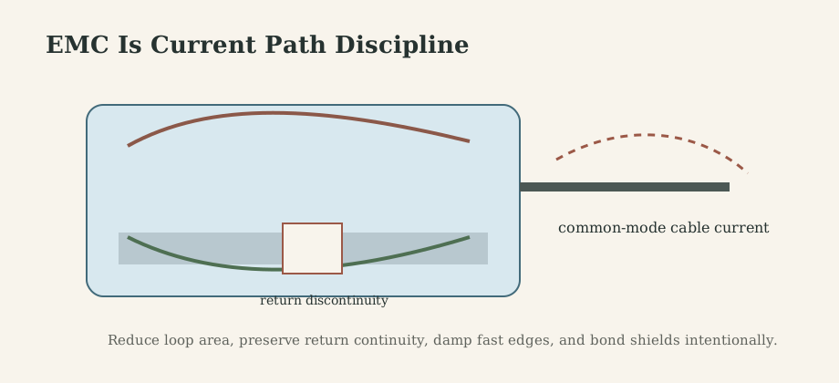
Reliability links electronics to mechanics and environment. Thermal cycling, vibration, moisture, contamination, connector strain, and derating policy shape field life. A release checklist should include functionality across temperature, power transients, EMC margin, calibration retention, clock/timing margin, and safe-state behavior on detected faults.
What This Framework Lets Us Do
Electronics gives the physical interface between computation and the world: sensing, amplification, conversion, actuation, communication, and power. A good design keeps equations, layout, thermal behavior, software timing, and validation evidence connected.
Where the Framework Stops Being Reliable
Hand calculations and ideal models are first-pass tools. Final confidence requires simulation, tolerance analysis, layout review, bench measurement, environmental tests, and failure-mode thinking. Datasheet typical values are not release guarantees.
Where the Subject Leads Next
The natural next steps are analog IC design, power electronics, embedded systems, FPGA design, RF engineering, instrumentation, EMC engineering, and hardware reliability.
Technical and Editorial Audit
- Compressed a long electronics survey into a device-to-system engineering note.
- Preserved EE2005 course attribution in the main text.
- Added original figures for the design stack, device-model hierarchy, analog signal chain, timing/conversion boundary, and EMC return paths.
- Kept key equations for circuit modeling, devices, amplification, converters, power stages, timing, and EMC.
- Datasheet-specific limits, safety margins, and compliance requirements must be verified for the target hardware.
Main Sources Used in This Note
- P. Horowitz and W. Hill, The Art of Electronics.
- A. S. Sedra and K. C. Smith, Microelectronic Circuits.
- R. C. Dorf and J. A. Svoboda, Introduction to Electric Circuits.
- H. W. Ott, Electromagnetic Compatibility Engineering.
- R. W. Erickson and D. Maksimovic, Fundamentals of Power Electronics.